
HCHiP Industry Training Courses Launch in November
We are pleased to announce that the industry training courses offered by the HCHiP project (Hungarian Chips Competence Centre) will begin in November 2026. The programme is primarily aimed at professionals from Hungarian small and medium-sized enterprises (SMEs) who wish to acquire up-to-date knowledge and practical experience in the semiconductor industry, electronics, microtechnologies, and related fields. All courses combine theoretical and practical components, allowing participants not only to learn the fundamentals of the technologies covered but also to gain hands-on experience with their applications using state-of-the-art laboratory equipment and methods. The courses will be delivered in one- or two-day formats.
Participation in HCHiP training courses is free of charge for professionals from Hungarian SMEs, but prior registration is required. Registration is only valid once confirmed by the organisers via email. An exception applies to the course entitled “Atomic-Level Structural Characterisation of Your Own Sample”, which includes the preparation and analysis of samples provided by participants. For this course, participants are required to pay a cost-based contribution depending on the sample being examined. Language of instruction: Hungarian.
We look forward to receiving your registration!
Our training programme:
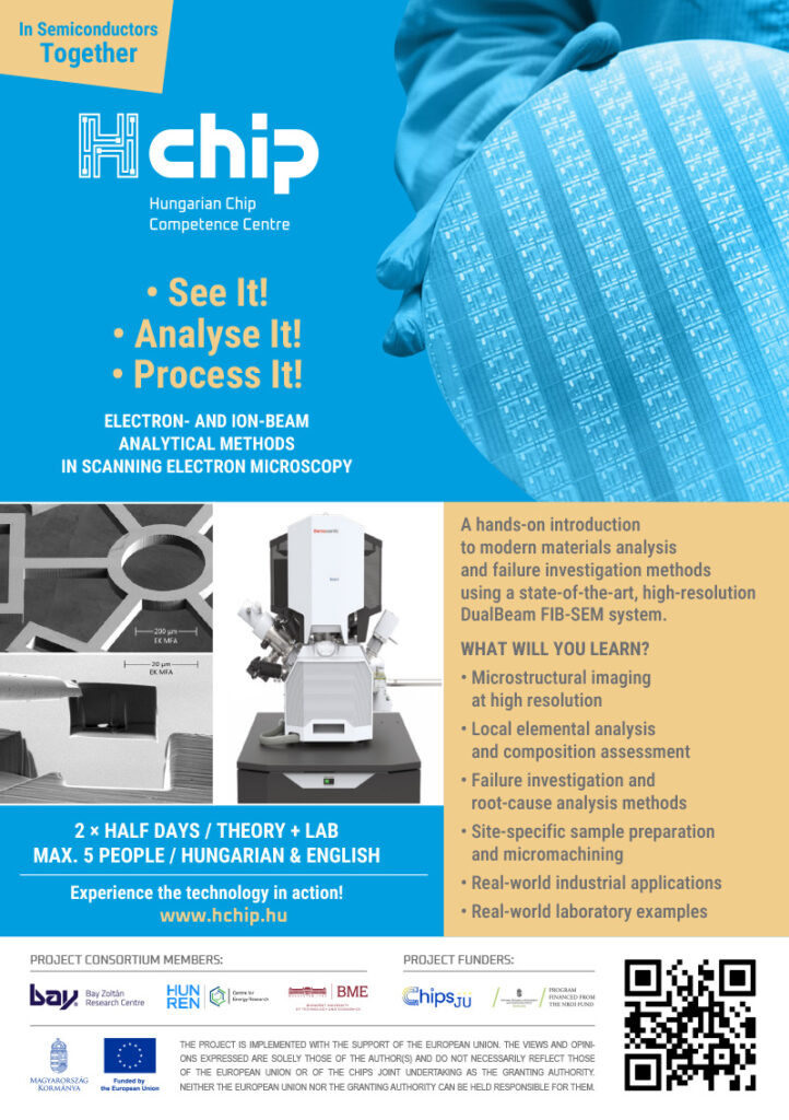
Electron and Ion Beam
Analytical Methods
in Scanning Electron
Microscopy
Participation requirements and registration
are available at the following links:
10 November 2026 ( https://luma.com/ra2j494o )
1-2 December 2026 ( https://luma.com/6fodtubt )
12 January 2027 ( https://luma.com/urd9yqqn )
| Duration | 1 day |
| Structure | Half-day theoretical training + half-day laboratory demonstration |
| Recommended group size | Maximum 5 participants |
| Target audience | Professionals from companies interested in the technology |
| Location | HUN-REN Energiatudományi Kutatóközpont, Műszaki Fizikai és Anyagtudományi Intézet, 1121 Budapest, Konkoly-Thege Miklós út 29-33. |
| Language of instruction | Hungarian |
Training Objective
The training provides participants with a comprehensive overview of modern scanning electron microscopy (SEM) investigation and microanalytical methods, as well as focused ion beam technologies, including their capabilities, limitations, and application areas. Participants will learn about techniques widely used in materials characterization, semiconductor technology, failure analysis, quality control, and research and development, and gain insight into how these technologies can support their own professional activities.
Theoretical Training (Half Day)
The theoretical module introduces the operating principles of the scanning electron microscope, the structure of electron-optical systems, fundamentals of vacuum technology, and the information obtained from interactions between the primary beam and the sample. Participants will learn the basics of secondary and backscattered electron imaging, contrast mechanisms, factors affecting resolution and image quality, and the correct interpretation of measurement results. Special emphasis is placed on energy-dispersive X-ray spectroscopy (EDS), including the capabilities and limitations of elemental analysis, the fundamentals of qualitative and quantitative analysis, and practical applications of elemental mapping. The course also discusses the information content of different analytical signals, spatial resolution considerations, and the types of information obtainable with various examination modes. In addition, participants are introduced to focused ion beam (FIB) technology, ion-sample interactions, ion microscopy, localized material processing, cross-section preparation, and targeted sample preparation. Topics also include gas injection systems (GIS), localized deposition of conductive and insulating layers, gas-assisted etching, and potential applications of nanomanipulators. The module further addresses practical limitations such as charging, contamination, sample damage, and the industrial relevance and typical applications of these technologies.
Laboratory Demonstration (Half Day)
The laboratory session builds directly on the concepts presented during the theoretical training. Participants will observe the operation of a scanning electron microscope and associated analytical systems using a state-of-the-art high-resolution DualBeam FIB-SEM platform, gaining insight into the practical aspects of sample preparation, measurement execution, and result evaluation. Through real-world examples, the demonstration illustrates how these technologies can be effectively applied to solve industrial challenges.
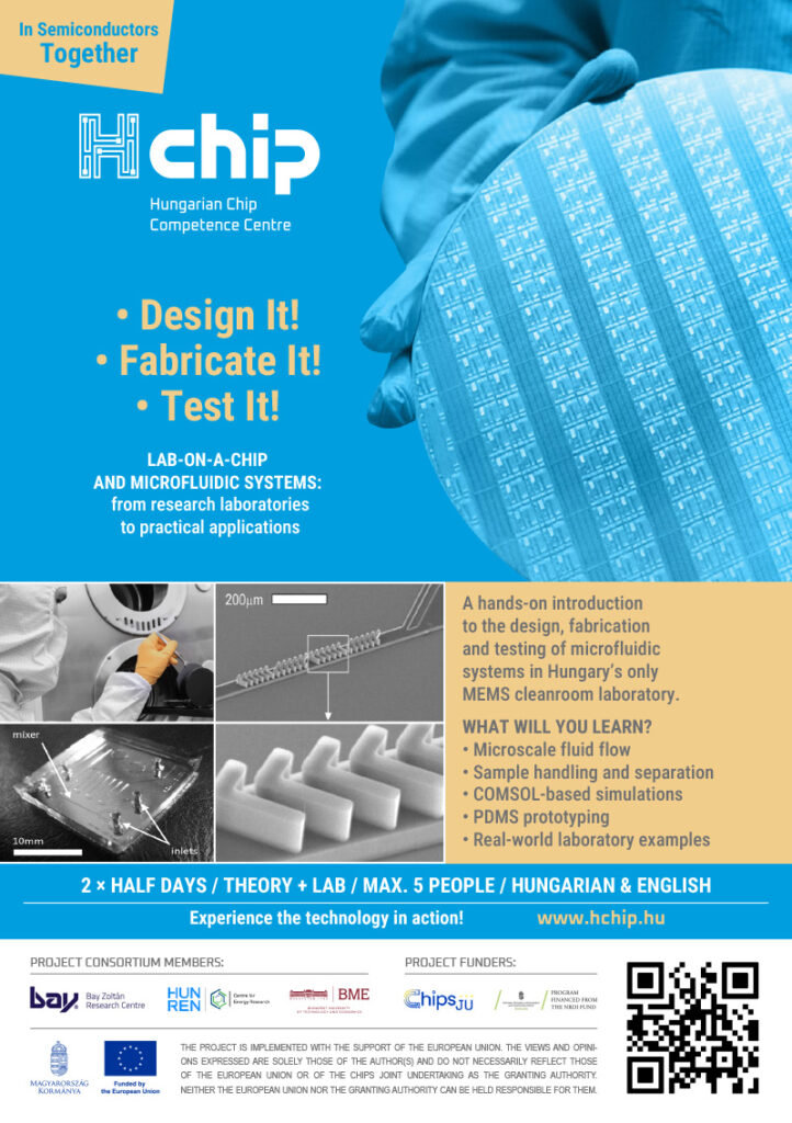
Lab-on-a-Chip and Microfluidic
Systems: From Research Laboratories
to Practical Application
Participation requirements and registration are available at the following links:
19-20 November 2026
(Session 1: https://luma.com/gnf7ypy1, Session 2: https://luma.com/e1kdje6k )
10-11 December 2026
(Session 1: https://luma.com/wuw1l1z5, Session 2: https://luma.com/4iesppdx )
14-15 January 2027
(Session 1: https://luma.com/7s880fun, Session 2: https://luma.com/i2yfi8j8 )
| Duration | 1 day |
| Structure | Half-day theoretical training + half-day laboratory demonstration |
| Recommended group size | Maximum 5 participants |
| Target audience | Professionals from companies interested in the technology |
| Location | HUN-REN Energiatudományi Kutatóközpont, Műszaki Fizikai és Anyagtudományi Intézet, 1121 Budapest, Konkoly-Thege Miklós út 29-33. |
| Language of instruction | Hungarian |
Training Objective
The training provides participants with a comprehensive understanding of Lab-on-a-Chip and microfluidic systems, including their operating principles, design considerations, manufacturing technologies, and application areas. Participants will learn how liquids, particles, and biological samples can be precisely manipulated at the micrometer scale and how these solutions are applied in diagnostic, pharmaceutical, biotechnological, and chemical microsystems. The course also presents the complete development workflow of microfluidic devices, from design and simulation through fabrication to experimental validation.
Theoretical Training (Half Day)
The theoretical module introduces the core concepts, operating principles, and application areas of Lab-on-a-Chip and microfluidic systems. Participants will learn the fundamentals of microscale fluid flow, the characteristics of laminar flow, and key physical phenomena governing microfluidic design, including the relevance of Reynolds and capillary numbers. The course covers passive and active approaches to sample transport and manipulation, mixing, separation, and particle and cell handling. It also presents the basics of finite element modeling (FEM) and the role of microfluidic simulations in COMSOL Multiphysics. Manufacturing technologies are discussed in detail, with emphasis on soft lithography, rapid prototyping using PDMS, as well as advanced approaches such as silicon-glass systems, deep reactive ion etching (DRIE), and bonding technologies. The advantages, limitations, and industrial applicability of each technology are also reviewed.
Laboratory Demonstration (Half Day)
The laboratory session takes place in Hungary’s only MEMS cleanroom facility and builds directly on the topics covered during the theoretical training. Participants gain insight into the fabrication and testing of microfluidic systems and become familiar with the key stages of prototyping and functional verification. The demonstration showcases technologies used in the production of PDMS-based microfluidic devices and experimental methods for investigating microfluidic phenomena and device performance. The objective of the laboratory module is to provide first-hand exposure to the practical aspects of developing, manufacturing, and experimentally evaluating microfluidic systems.
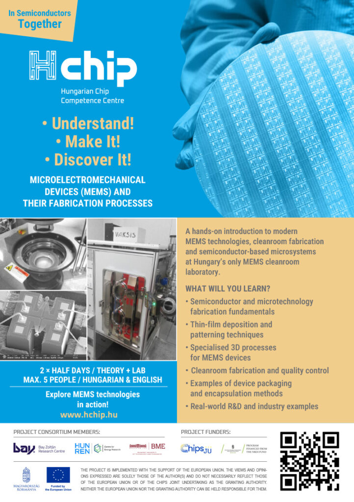
Micro-ElectroMechanical
Systems (MEMS)
and their processing
technology
Participation requirements and registration
are available at the following links:
10 November 2026 ( https://luma.com/bmp65rf2 )
8 December 2026 ( https://luma.com/fdg1xzhv )
12-13 January 2027 ( https://luma.com/zodtk99f )
| Duration | 1 day |
| Structure | Half-day theoretical training + half-day laboratory demonstration |
| Recommended group size | Maximum 5 participants |
| Target audience | Professionals from companies interested in the technology |
| Location | HUN-REN Energiatudományi Kutatóközpont, Műszaki Fizikai és Anyagtudományi Intézet, 1121 Budapest, Konkoly-Thege Miklós út 29-33. |
| Language of instruction | Hungarian |
Training Objective
During this one-day training session, we will provide an introductory overview of modern microelectronics and microtechnology processes. We will demonstrate how — much like the manufacturing of integrated circuits — microscale sensors and actuators (Micro Electro-Mechanical Systems, MEMS), produced in large quantities at extremely low cost, have become an integral part of our everyday lives to an incredible extent. Using a few examples, we will illustrate the important role they play in modern industrial and agricultural production, as well as in rapidly advancing medical and surgical procedures. The goal of the course is to provide an impression into one of the most dynamically developing industries of our time, to highlight its inherent potential, and — through specific in-house developments — to show the R&D activities of the Microsystems and Nanostructures Laboratories at the Energy Research Centre and the opportunities they offer.
Theoretical Training (Half Day)
During the theoretical training, we provide a brief overview of the main steps in MEMS manufacturing, primarily based on the manufacturing technology of silicon integrated circuits; We cover thin-film deposition, patterning, and thin-film removal techniques, as well as methods for modifying the electrical properties of semiconductors. We also pay special attention to the specialized 3D processes used in the fabrication of MEMS devices. We will discuss the relationships between technology and air cleanness as well as the purity of processing materials. We will emphasize the importance of precision and reproducibility in each processing step to ensure that, at the end of this complex technological process, we achieve adequate yield and produce integrated circuits and MEMS devices of reliable quality. In addition to the front-end silicon wafer processing techniques listed above, we will also briefly discuss chip encapsulation and packaging techniques, which often play a decisive role in sensor devices that measure signals of the environment.
Laboratory Demonstration (Half Day)
During the laboratory program, we will show the institute’s micro- and nanotechnology cleanrooms, as well as the basic manufacturing equipment discussed in the lectures. In addition to the tour, we will also provide an opportunity to create a micro-sample using thin-film patterning, thereby offering a taste of excitement and beauty of manufacturing technology.
Structural
investigation
on atomic level
Participation requirements and registration
are available at the following links:
13 November 2026 ( https://luma.com/ib241r61 )
4 December 2026 ( https://luma.com/4amlxnxk )
28 January 2027 ( https://luma.com/6quyufay )
| Duration | 1 day |
| Structure | 2 x 45 min theoretical training + 2 x 3h laboratory demonstration |
| Recommended group size | Maximum 5 participants |
| Target audience | Professionals from companies interested in the technology |
| Location | HUN-REN Energiatudományi Kutatóközpont, Műszaki Fizikai és Anyagtudományi Intézet, 1121 Budapest, Konkoly-Thege Miklós út 29-33. |
| Language of instruction | Hungarian |
Training Objective
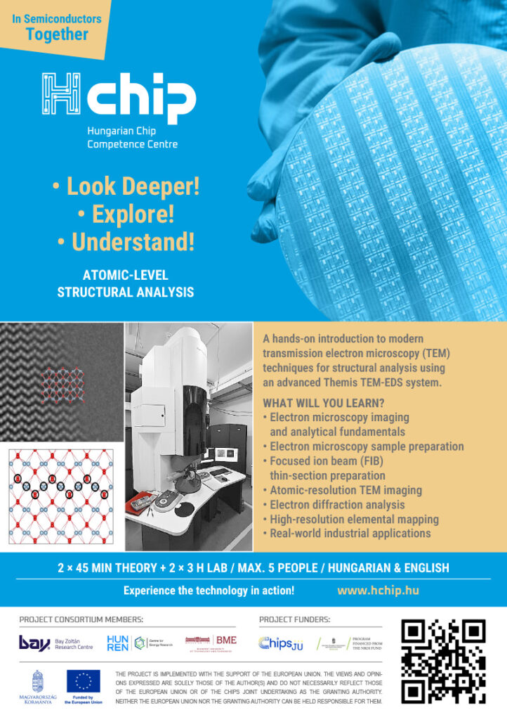
The aim of this introductory course is to present the capabilities of the transmission electron microscopy in structural characterization and analysis. Depending on the participants’ interests and fields of expertise, the course will explore the potential applications of electron microscopy in manufacturing, research, and development. It will also introduce the support opportunities provided by the HChip project and Hungary’s electron microscopy laboratories, highlighting their role in facilitating access to advanced microscopy infrastructure, technical expertise, and collaborative research services.
Theoretical Training (2 x 45 min)
The lectures provide an overview of the major electron microscopy techniques, including scanning electron microscopy (SEM), transmission electron microscopy (TEM), scanning transmission electron microscopy (STEM), and the principal methods of specimen preparation. Following the lectures, participants will take part in laboratory sessions demonstrating the preparation of thin lamellae using focused ion beam (FIB) technology. The prepared specimens will then be examined by transmission electron microscopy to acquire atomic-resolution images, electron diffraction patterns, and high-resolution elemental maps, illustrating the capabilities of advanced electron microscopy for structural and compositional characterization. A shortened version of the course can also be delivered at an external venue. In this format, only the lecture component is offered, and no participant limit applies.
Laboratory Demonstration (2x 3h)
The laboratory programme builds on the theoretical concepts presented during the lectures. Participants will gain first-hand experience of the operation of a transmission electron microscope and its associated analytical systems using a state-of-the-art, high-resolution Thermo Scientific Themis TEM equipped with energy-dispersive X-ray spectroscopy (EDS). The practical sessions provide insight into the complete workflow of electron microscopy, including specimen preparation, data acquisition, and the evaluation and interpretation of results. Throughout the laboratory demonstration, real-world case studies will illustrate how the presented techniques can be applied to address industrial challenges and support manufacturing, quality control, and research and development activities.
Structural
investigation
on atomic level
with own sample
Participation requirements and registration
are available at the following link:
2026. december 3. ( https://luma.com/rbm6kaxa )
| Duration | 1 day |
| Structure | 2 x 45 min theoretical training + laboratory demonstration |
| Recommended group size | Maximum 5 participants |
| Target audience | Professionals from companies interested in the technology |
| Location | HUN-REN Energiatudományi Kutatóközpont, Műszaki Fizikai és Anyagtudományi Intézet, 1121 Budapest, Konkoly-Thege Miklós út 29-33. |
| Language of instruction | Hungarian |
Training Objective
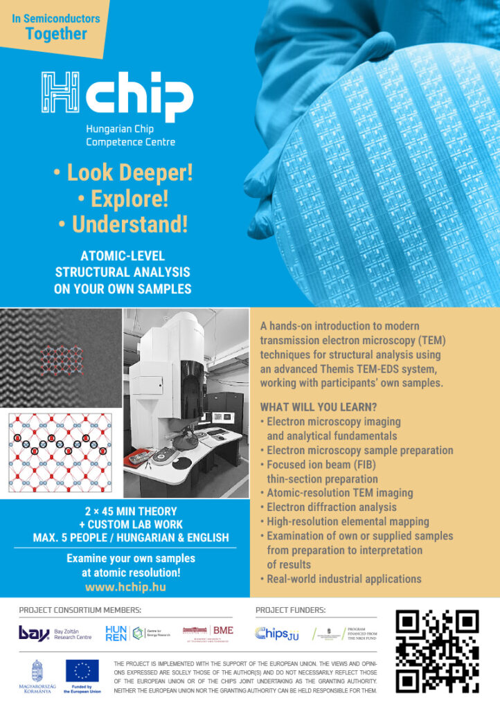
The aim of this introductory course is to present the capabilities of the transmission electron microscopy in structural characterization and analysis. Depending on the participants’ interests and fields of expertise, the course will explore the potential applications of electron microscopy in manufacturing, research, and development. It will also introduce the support opportunities provided by the HChip project and Hungary’s electron microscopy laboratories, highlighting their role in facilitating access to advanced microscopy infrastructure, technical expertise, and collaborative research services.
Theoretical Training (2 x 45 min)
The lectures provide an overview of the major electron microscopy techniques, including scanning electron microscopy (SEM), transmission electron microscopy (TEM), scanning transmission electron microscopy (STEM), and the principal methods of specimen preparation. Following the lectures, participants will take part in laboratory sessions demonstrating the preparation of thin lamellae using focused ion beam (FIB) technology. The prepared specimens will then be examined by transmission electron microscopy to acquire atomic-resolution images, electron diffraction patterns, and high-resolution elemental maps, illustrating the capabilities of advanced electron microscopy for structural and compositional characterization. A shortened version of the course can also be delivered at an external venue. In this format, only the lecture component is offered, and no participant limit applies.
Laboratory Demonstration
Participants may bring their own samples for analysis or choose from samples provided by the laboratory. The programme offers a comprehensive demonstration of the complete electron microscopy workflow, from specimen preparation to data acquisition, analysis, and interpretation of the results. The laboratory sessions build on the theoretical concepts introduced during the lectures. Participants will gain first-hand experience of the operation of a transmission electron microscope and its associated analytical systems using a state-of-the-art, high-resolution Thermo Scientific Themis TEM equipped with energy-dispersive X-ray spectroscopy (EDS). The practical sessions provide insight into the preparation of specimens, instrument operation, data collection, and the evaluation and interpretation of microscopy results. Throughout the demonstration, real-world case studies will illustrate how advanced electron microscopy techniques can be applied to solve industrial problems and support manufacturing, quality control, failure analysis, and research and development activities.